

Core Labs
Advanced Light Microscopy / Spectroscopy (ALMS)
Advanced Light Microscopy / Spectroscopy (ALMS)
Shimon Weiss, Faculty Director
Laurent A. Bentolila, Scientific Director
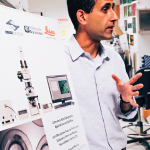
Advanced Light Microscopy/Spectroscopy Shared Facility provides researchers with cutting edge techniques to allow for the structural and kinetic studies of a myriad of macromolecules. This facility utilizes techniques such as spectroscopy and image analysis by using fluorescent semiconductor crystals and quantum dots to image these macromolecules.
Electron Imaging Center for NanoMachines (EICN)
Electron Imaging Center for NanoMachines (EICN)
Z. Hong Zhou, Faculty Director
Xing Zhang, Technical Director
Ivo Atanasov, Associate Director
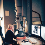
The Electron Imaging Center for Nanomachines (EICN) allows researchers to image a range of substances in 3D at high magnification. It’s focused on comprehending the mechanisms of life’s workhorse: proteins. The facility includes single particle cryo-electron microscopy (cryoEM) at near atomic resolution, and cryo-electron tomography (cryoET) at molecular resolution, high-resolution transmission electron microscopy (TEM), as well as scanning transmission electron microscopy (STEM) and energy dispersive X-ray (EDX) analysis for mass and elementary mapping.
Integrated Systems Nanofabrication Cleanroom (ISNC)
Integrated Systems Nanofabrication Cleanroom (ISNC)
Aydogan Ozcan, Faculty Director
Adam Stieg, Interim Technical Director
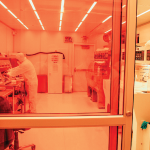
The CNSI ISNC consists of 8,900 square feet of vertical-flow clean room space and 680 square feet of purified air, and provides facilities for chemists, biologists, doctors and engineers to work with DNA, biological molecules, and for more traditional nano-device fabrication.
Nano and Pico Characterization Lab
Nano and Pico Characterization Lab
nanopicolab.cnsi.ucla.edu/pages/homepage
James Gimzewski, Faculty Director
Adam Stieg, Scientific Director
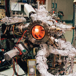
The Nano and Pico Characterization Lab (NPC) at CNSI provides access to state-of-the-art methods toward the characterization of surfaces, adsorbates, nanostructures, and devices through the use of Scanning Probe Microscopy (SPM). The facility includes Scanning Tunneling Microscopy (STM) and Atomic Force Microscopy (AFM).
* Art|Sci has access to these facilities with prior arrangements on a case by case basis.